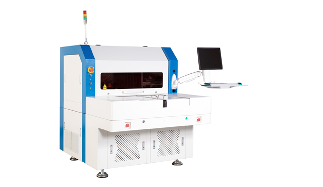
DirectLaser PC6- High-End PCB Laser Structuring Equipment
Based on DCT S&S technology, DirectLaser PC6 could process an 80mm x 100mm conductive pattern on PCB in just a few minutes. The system could also have drilling and Routing functions when it equipped with green, UV, picosecond, or femtosecond ultrashort pulse laser source. In this way, in addition to the hole metallization and lamination process, making PCB easily like printing on a single machine is realizabl.
S&S direct laser circuit technology could ensure wire geometric error of 5 micron or even 3 microns, and keep the original copper surface clean, especially suitable for making impedance, high-speed IF, microwave circuits, and other expensive, special demand high-end PCBs. There is no need to use optical mask or other tools to do the drawing Shape transfer, no chemicals, no chemical-related pre-treatment and post-treatment process. The innovative S&S direct laser circuit technology with the feature of precision, accurate, simple, flexible, and environment friendly make circuit manufacturing quality, efficiency and cost advantages.
Features
Data driven
System
Device
Stripping
Software
Product parameters
Technical data | DirectLaser PC6 |
Working area | 533mm x 610mm |
Wave length | 1,064nm/532nm/355nm |
Minimum gap | 25μm* |
Mimimum track | 20μm* |
Processing speed | 25cm2/min* |
Repeat postioning accuacy | ±2μm |
Resolution scan field | ≤1μm |
X/Y step resolution | 0.5μm |
Weight | Approx. 1,700kg |
Dimension(W x H x D) | 1,400mm x 1,750mm x 1,600mm |
Data acceptance | Gerber, HPGL, Sieb & Meier, Excellon, ODB++ |
Matching and Options | DirectLaser PC6 |
Data processing software | CircuitCAM 7 LaserPlus |
System operating software | DreamCreaTor 3 |
Dust exhaust system | 210m?/hr,220VAC,1.3kW |
Postioning | Automatic CCD camera fiducial positioning |
Work piece fixation | Vacuum absorbing platform |
Operation environment | DirectLaser PC6 |
Power supply | 380VAC/50Hz,3kW** |
Operation temperature | 26°C±4°C |


